Guidelines for designers#
This development board utilizes XMOS’s XU316-1024-QF60A processor.
The datasheet for XU316-1024-QF60A ia available to Download
Note
The XU316-1024-QF60A is a 1v8 IO device. This development kit makes use of level translators to connect to the 3v3 Raspberry Pi interface. Depending on your requirements, you may prefer to use the XU316-1024-QF60B which offers 3v3.
A complete list of XMOS processors can be found Here
CAD & Design files#
The CAD design files are available to Download
This zip archive contains:
Altium CAD data
PCB, Assembly drawings & BOM
Schematics
XU316-1024-QF60A-C24 Pin assignment#
This development kit assumes that the XU316-1024-QF60A has been programmed to meet the following pin assignement:
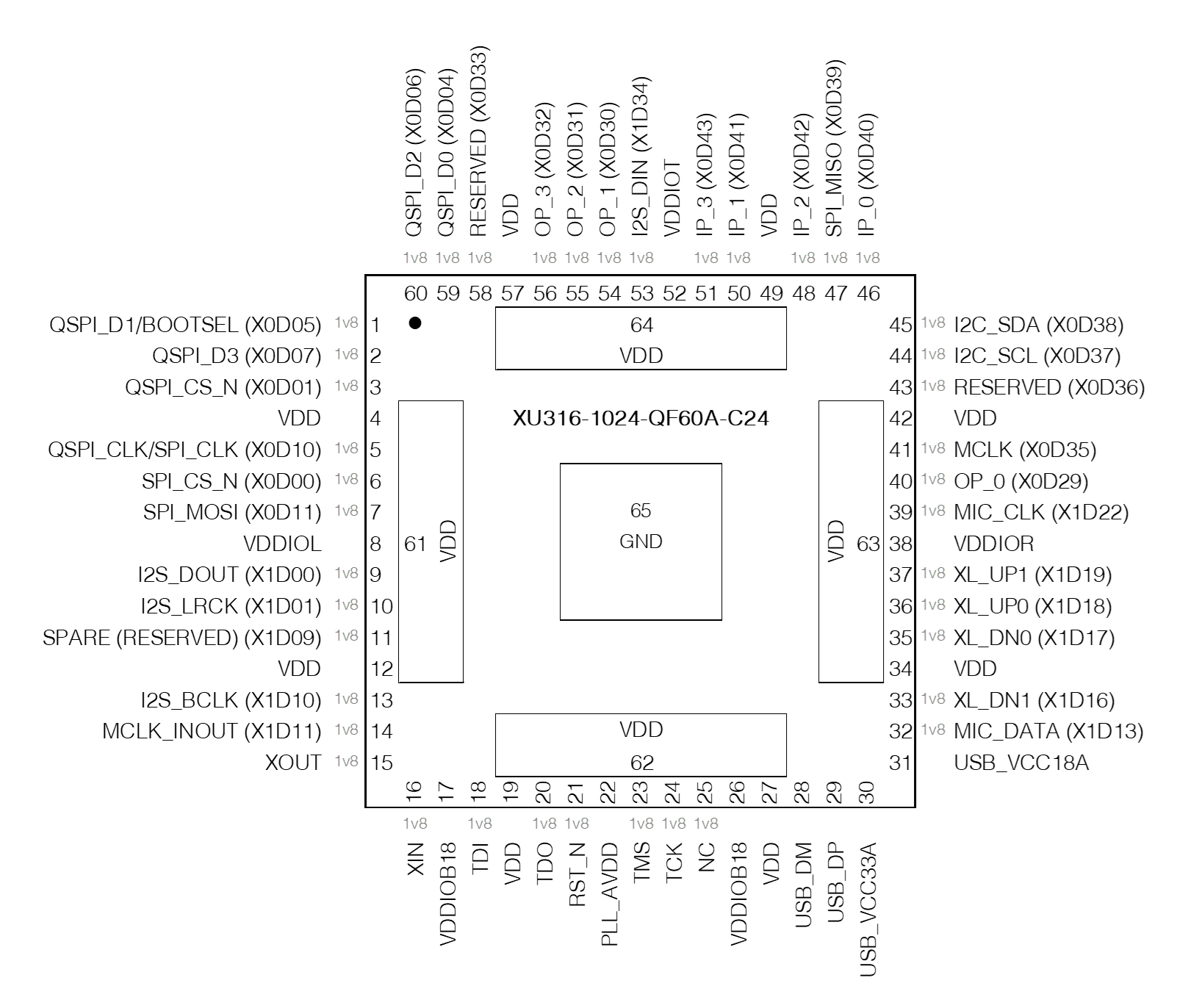
Fig. 5 XU316-1024-QF60A-C24 Pin assignment#
Port map#
Test Point J6#
Pin |
XU316 pin |
XU316 port |
Signal name |
XU316 usage |
Comments |
Direction w.r.t XU316 |
|---|---|---|---|---|---|---|
1 |
41 |
X0D35 |
MCLK |
Master audio clock |
I |
|
2 |
VDDIO |
|||||
3 |
GND |
|||||
4 |
13 |
X1D10 |
I2S_BCLK |
I2S bit synchronisation clock |
Configurable for 16KHz (1.024MHz) and 48KHz (3.072MHz) sample rates |
O (master), I (slave) |
5 |
10 |
X1D01 |
I2S_LRCK |
I2S Left/Right clock |
48kHz or 16KHz clock derived as I2S_BLCK/64. |
O (master), I (slave) |
6 |
9 |
X1D00 |
I2S_DOUT |
I2S Data Out |
Audio data out to host processor |
O |
7 |
53 |
X1D34 |
I2S_DIN |
Peripheral I2S interface - I2S data input |
I |
|
8 |
GND |
|||||
9 |
7 |
X0D11 |
SPI_MOSI |
SPI Master Out Slave In |
I |
|
10 |
6 |
X0D00 |
SPI_CS_N |
Slave SPI boot / Peripheral SPI Master Chip Select |
Pull high externally to the device using a 4.7k ohm resistor |
I |
11 |
5 |
X0D10 |
QSPI_CLK/ SPI_CLK |
QSPI Clock |
O |
|
12 |
47 |
X0D39 |
SPI_MISO |
SPI Master In Slave Out |
May be left floating if not required |
O |
13 |
GND |
|||||
14 |
1 |
X0D05 |
QSPI_D1/ BOOTSEL |
QSPI Data Line 1 and boot selection. |
If pin is tied high via a 4.7k ohm resistor on startup the device will start in SPI slave boot mode. If the pin is left floating or connected to a quad SPI D1 pin on a memory memory device, the device will start in QSPI master mode and attempt to boot from the QSPI flash memory. |
I / O |
15 |
40 |
X0D29 |
OP_0 |
General purpose output |
Eval kit - Used as interupt to the RaPi, via an I2C expander. |
O |
16 |
54 |
X0D30 |
OP_1 |
General purpose output |
Eval kit - LED_R |
O |
17 |
55 |
X0D31 |
OP_2 |
General purpose output |
Eval kit - LED_G |
O |
18 |
GND |
|||||
19 |
56 |
X0D32 |
OP_3 |
General purpose output |
Eval kit - Test point (and DAC reset if no-fit resistor fitted) |
O |
20 |
46 |
X0D40 |
IP_0 |
Eval kit Mute |
I |
|
21 |
50 |
X0D41 |
IP_1 |
Eval kit BUTTON |
I |
|
22 |
48 |
X0D42 |
IP_2 |
General purpose input |
I |
|
23 |
GND |
|||||
24 |
51 |
X0D43 |
IP_3 |
General purpose input |
I |
|
25 |
44 |
X0D37 |
I2C_SCL |
I2C serial clock line for receiving control command from I2C host |
I / O |
|
26 |
45 |
X0D38 |
I2C_SDA |
I2C serial data line for receiving control command from I2C host |
I / O |
|
Microphone connectors#
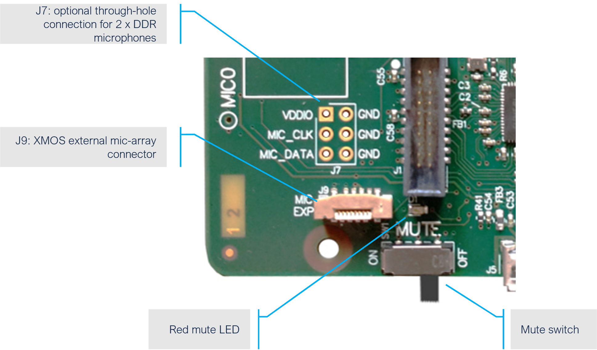
Fig. 6 Microphone options#
Note
When the mute switch is set to “mute” (Red LED On) then an external pair of DDR microphones may be connected to either of the test point or microphoone array connector.
Pin |
XU316 pin |
XU316 port |
Signal name |
XU316 usage |
Comments |
Direction w.r.t XU316 |
|---|---|---|---|---|---|---|
1 |
3 |
X0D01 |
QSPI_CS_N |
QSPI Boot Flash - Chip Select |
Pull high externally to the device using a 4.7k ohm resistor |
O |
2 |
VDDIO |
|||||
3 |
59 |
X0D04 |
QSPI_D0 |
QSPI Boot Flash / QSPI Data Line 0 |
I / O |
|
4 |
1 |
X0D05 |
QSPI_D1/ BOOTSEL |
QSPI Data Line 1 and boot selection. |
If pin is tied high via a 4.7k ohm resistor on startup the device will start in SPI slave boot mode. If the pin is left floating or connected to a quad SPI D1 pin on a memory memory device, the device will start in QSPI master mode and attempt to boot from the QSPI flash memory. |
I / O |
5 |
60 |
X0D06 |
QSPI_D2 |
QSPI Data Line 2 |
I / O |
|
6 |
2 |
X0D07 |
QSPI_D3 |
QSPI Data Line 3 |
I / O |
|
7 |
GND |
|||||
8 |
5 |
X0D10 |
QSPI_CLK/ SPI_CLK |
QSPI Clock |
O |
Pin |
XU316 pin |
XU316 port |
Signal name |
XU316 usage |
Comments |
Direction w.r.t XU316 |
|---|---|---|---|---|---|---|
1 |
VDDIO |
|||||
2 |
GND |
|||||
3 |
39 |
X1D22 |
MIC_CLK |
Microphone clock output. |
3.072MHz |
O |
4 |
GND |
|||||
5 |
32 |
X1D13 |
MIC_DATA |
PDM microphone input |
Note that this is a DDR input, permitting a pair of digital DDR microphones to share this input |
I |
6 |
GND |
|||||
7 |
NC |
|||||
8 |
NC |
XMOS Debug interface (J1)#
Pin |
XU316 pin |
XU316 port |
Signal name |
XU316 usage |
Comments |
Direction w.r.t XU316 |
|---|---|---|---|---|---|---|
1 |
1V8 |
|||||
2 |
23 |
TMS |
TMS |
JTAG test mode select |
This pin has a weak internal pull-up. See note on debug headers.. |
I |
3 |
GND |
|||||
4 |
24 |
TCK |
TCK |
JTAG test clock input |
This pin has a Schmitt trigger input and an internal weak pull-down. See note on debug headers. |
I |
5 |
GND |
|||||
6 |
20 |
TDO |
TDO |
JTAG test data output |
See note on debug headers. |
O |
7 |
GND |
|||||
8 |
18 |
TDI |
TDI |
JTAG test data input |
This pin has a weak internal pull-up. See note on debug headers. |
I |
9 |
GND |
|||||
10 |
21 |
RST_N |
RST_N |
Device reset |
Active low. This pin has a Schmitt trigger input and an internal weak pull up |
I |
11 |
VDDIO |
|||||
12 |
33 |
X1D16 |
XL_DN1 |
XLINK |
These 4 signals form a single 2-wire xlink connection for advanced debug only. Do not connect in production desings. |
I |
13 |
GND |
|||||
14 |
35 |
X1D17 |
XL_DN0 |
XLINK |
I |
|
15 |
GND |
|||||
16 |
36 |
X1D18 |
XL_UP0 |
XLINK |
O |
|
17 |
GND |
|||||
18 |
37 |
X1D19 |
XL_UP1 |
XLINK |
O |
|
19 |
GND |
|||||
20 |
NC |
Raspberry Pi host interface (J4)#
Raspberry Pi |
Signal |
Pin |
Pin |
Signal |
Raspberry Pi |
|---|---|---|---|---|---|
3V3 |
NC |
1 |
2 |
PI_5V |
5V |
GP2 |
PI_I2C_SDA |
3 |
4 |
PI_5V |
5V |
GP3 |
PI_I2C_SCL |
5 |
6 |
GND |
GND |
GP4 |
PI_MCLK |
7 |
8 |
NC |
GP14 |
GND |
GND |
9 |
10 |
NC |
GP15 |
GP17 |
NC |
11 |
12 |
PI_I2S_BCLK |
GP18 |
GP27 |
PI_INT_N |
13 |
14 |
GND |
GND |
GP22 |
NC |
15 |
16 |
NC |
GP23 |
3V3 |
NC |
17 |
18 |
NC |
GP24 |
GP10 |
PI_SPI_MOSI |
19 |
20 |
GND |
GND |
GP9 |
PI_SPI_MISO |
21 |
22 |
NC |
GP25 |
GP11 |
PI_SPI_CLK |
23 |
24 |
PI_SPI_CS_N |
GP8 |
GND |
GND |
25 |
26 |
NC |
GP7 |
ID_SD |
NC |
27 |
28 |
NC |
ID_SC |
GP5 |
NC |
29 |
30 |
GND |
GND |
GP6 |
NC |
31 |
32 |
NC |
GP12 |
GP13 |
NC |
33 |
34 |
GND |
GND |
GP19 |
PI_I2S_LRCK |
35 |
36 |
NC |
GP16 |
GP26 |
NC |
37 |
38 |
PI_I2S_DIN |
GP20 |
GND |
GND |
39 |
40 |
PI_I2S_DOUT |
GP21 |
Flash Test Point (J8)#
Pin |
XU316 pin |
XU316 port |
Signal name |
XU316 usage |
Comments |
Direction w.r.t XU316 |
|---|---|---|---|---|---|---|
1 |
3 |
X0D01 |
QSPI_CS_N |
QSPI Boot Flash - Chip Select |
Pull high externally to the device using a 4.7k ohm resistor |
O |
2 |
VDDIO |
|||||
3 |
59 |
X0D04 |
QSPI_D0 |
QSPI Boot Flash / QSPI Data Line 0 |
I / O |
|
4 |
1 |
X0D05 |
QSPI_D1/ BOOTSEL |
QSPI Data Line 1 and boot selection. |
If pin is tied high via a 4.7k ohm resistor on startup the device will start in SPI slave boot mode. If the pin is left floating or connected to a quad SPI D1 pin on a memory memory device, the device will start in QSPI master mode and attempt to boot from the QSPI flash memory. |
I / O |
5 |
60 |
X0D06 |
QSPI_D2 |
QSPI Data Line 2 |
I / O |
|
6 |
2 |
X0D07 |
QSPI_D3 |
QSPI Data Line 3 |
I / O |
|
7 |
GND |
|||||
8 |
5 |
X0D10 |
QSPI_CLK/ SPI_CLK |
QSPI Clock |
O |
Schematics#
These schematics are available in the CAD data, available to Download
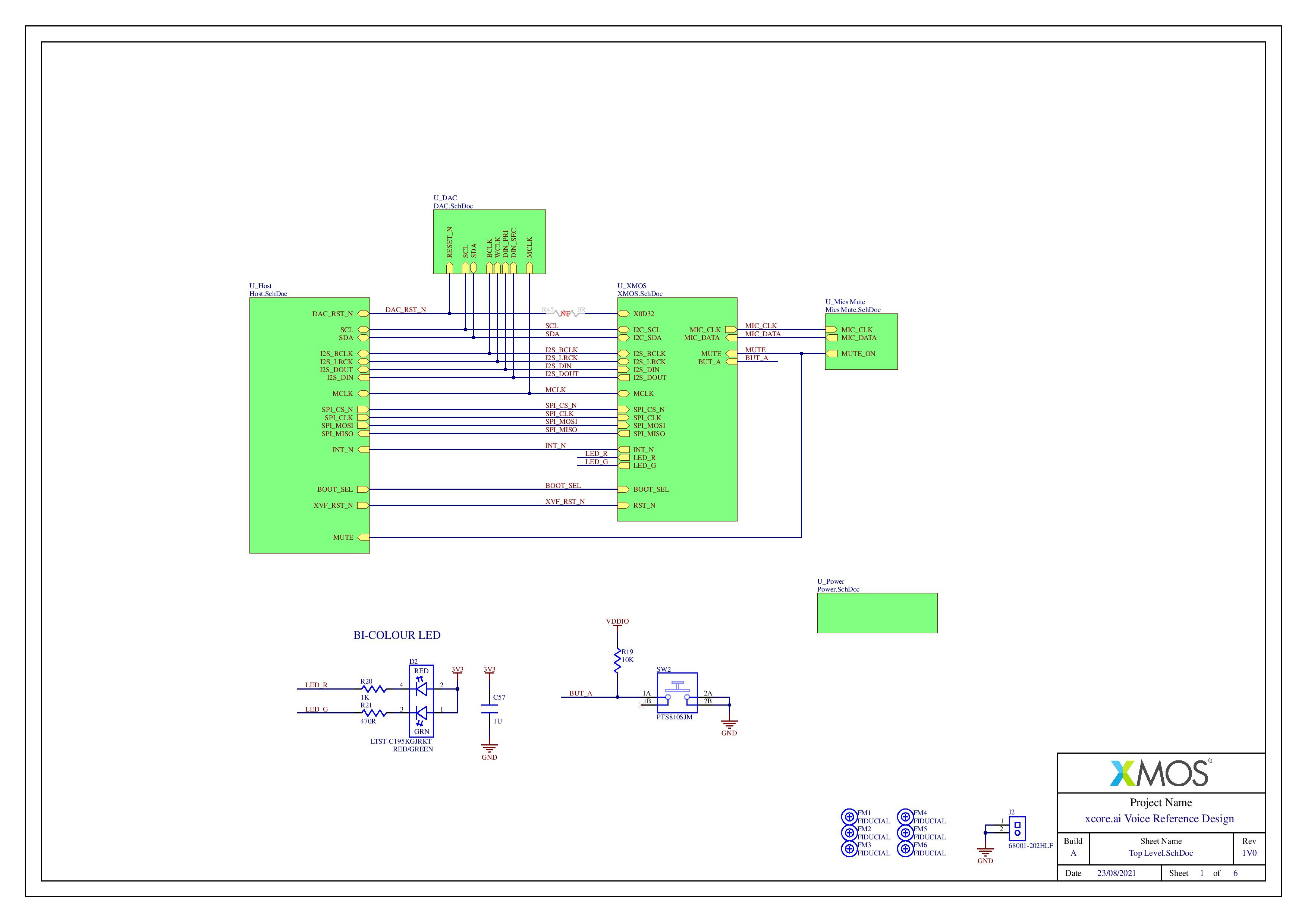
Fig. 7 XK-VOICE-L71 Schematic, page 1#
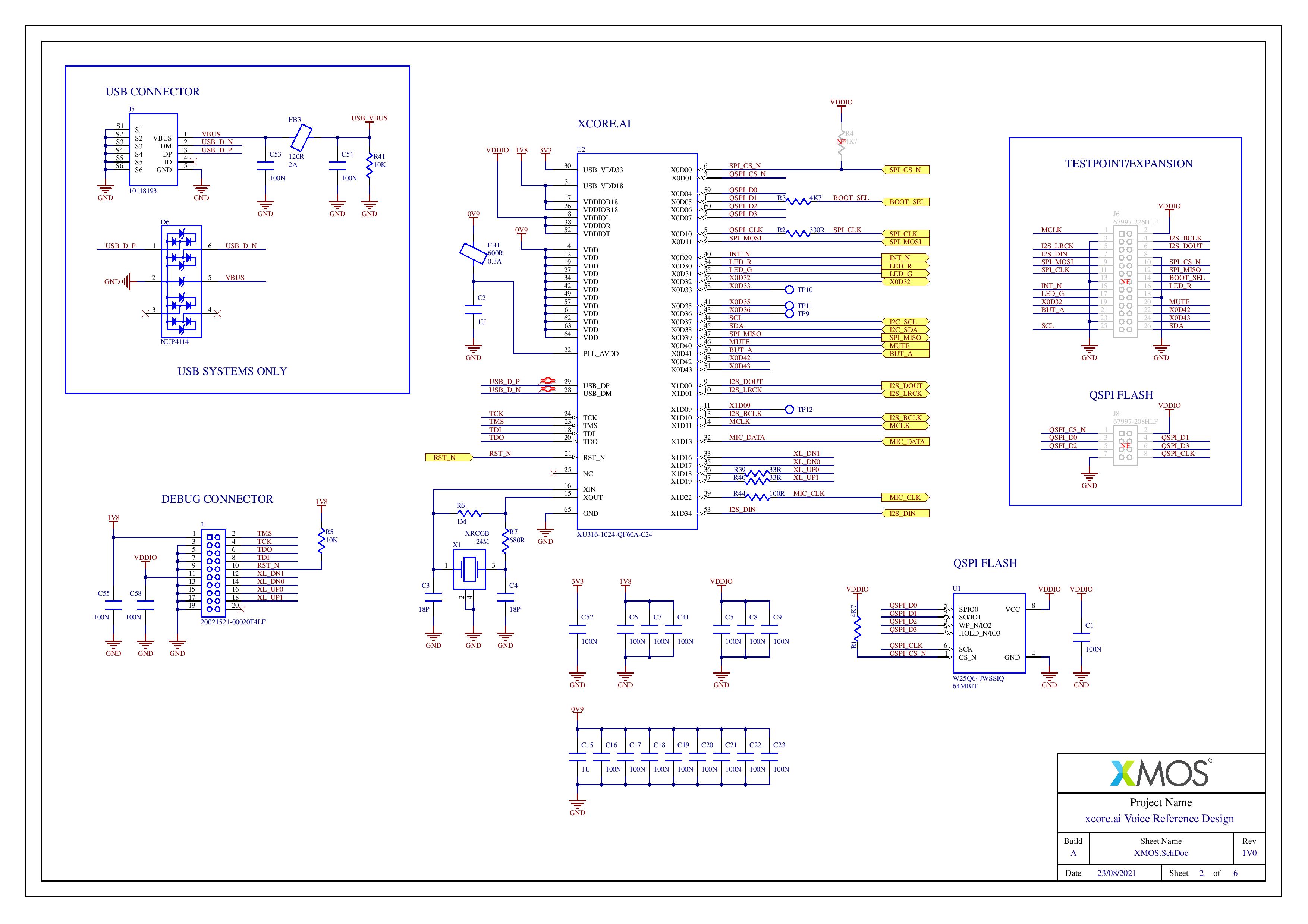
Fig. 8 XK-VOICE-L71 Schematic, page 2#
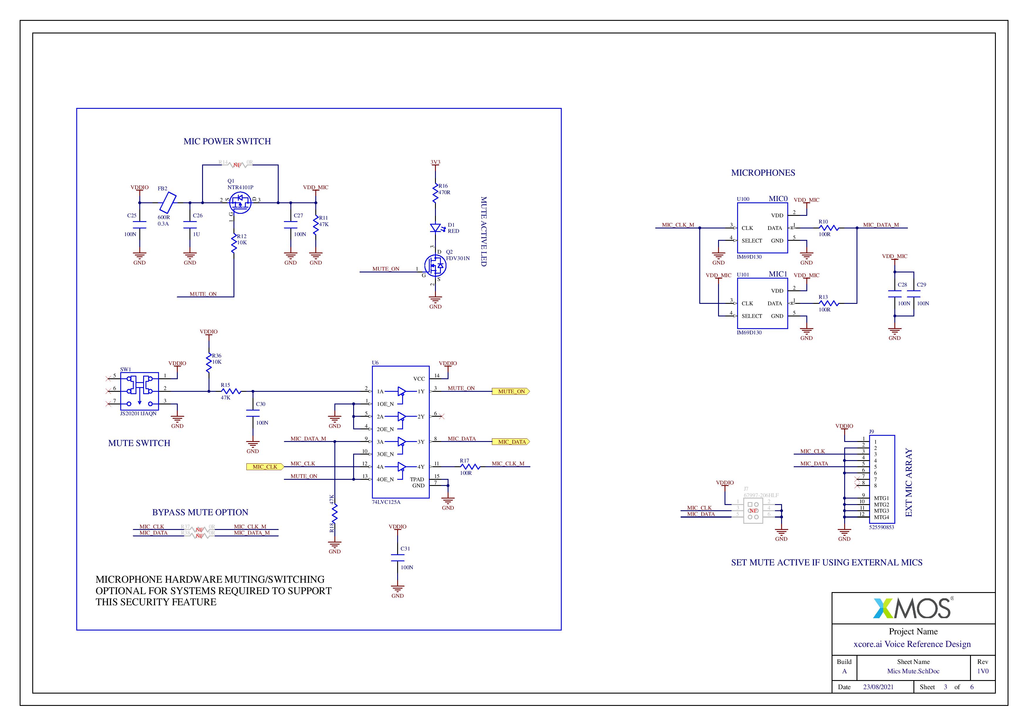
Fig. 9 XK-VOICE-L71 Schematic, page 3#
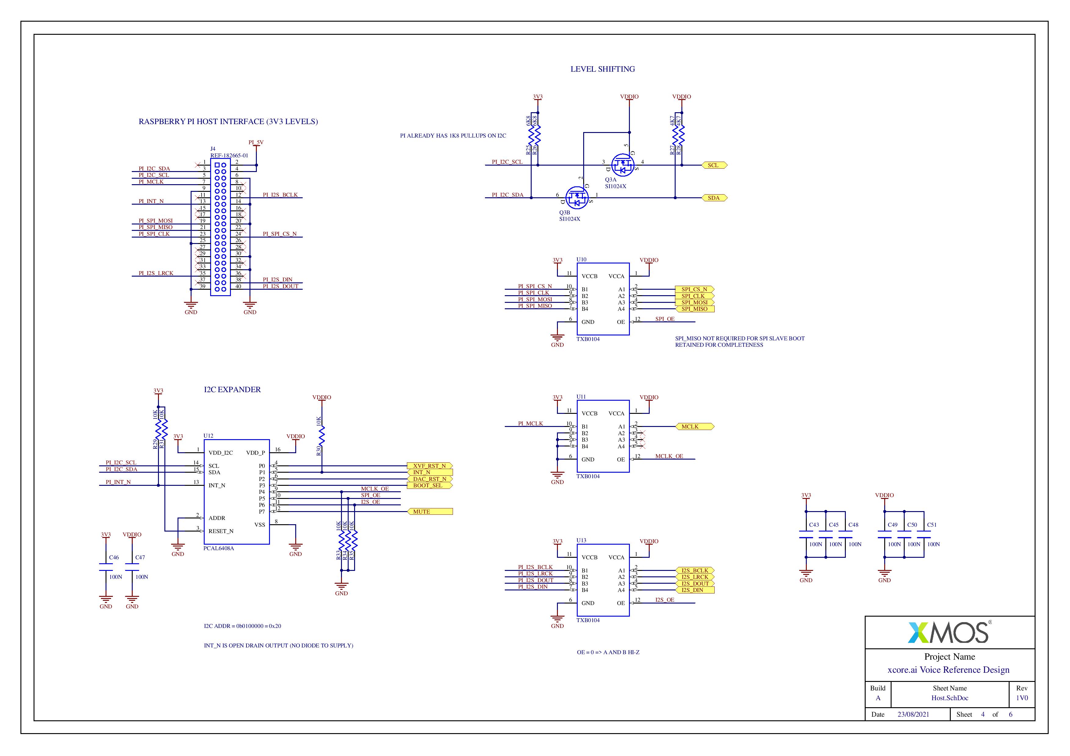
Fig. 10 XK-VOICE-L71 Schematic, page 4#
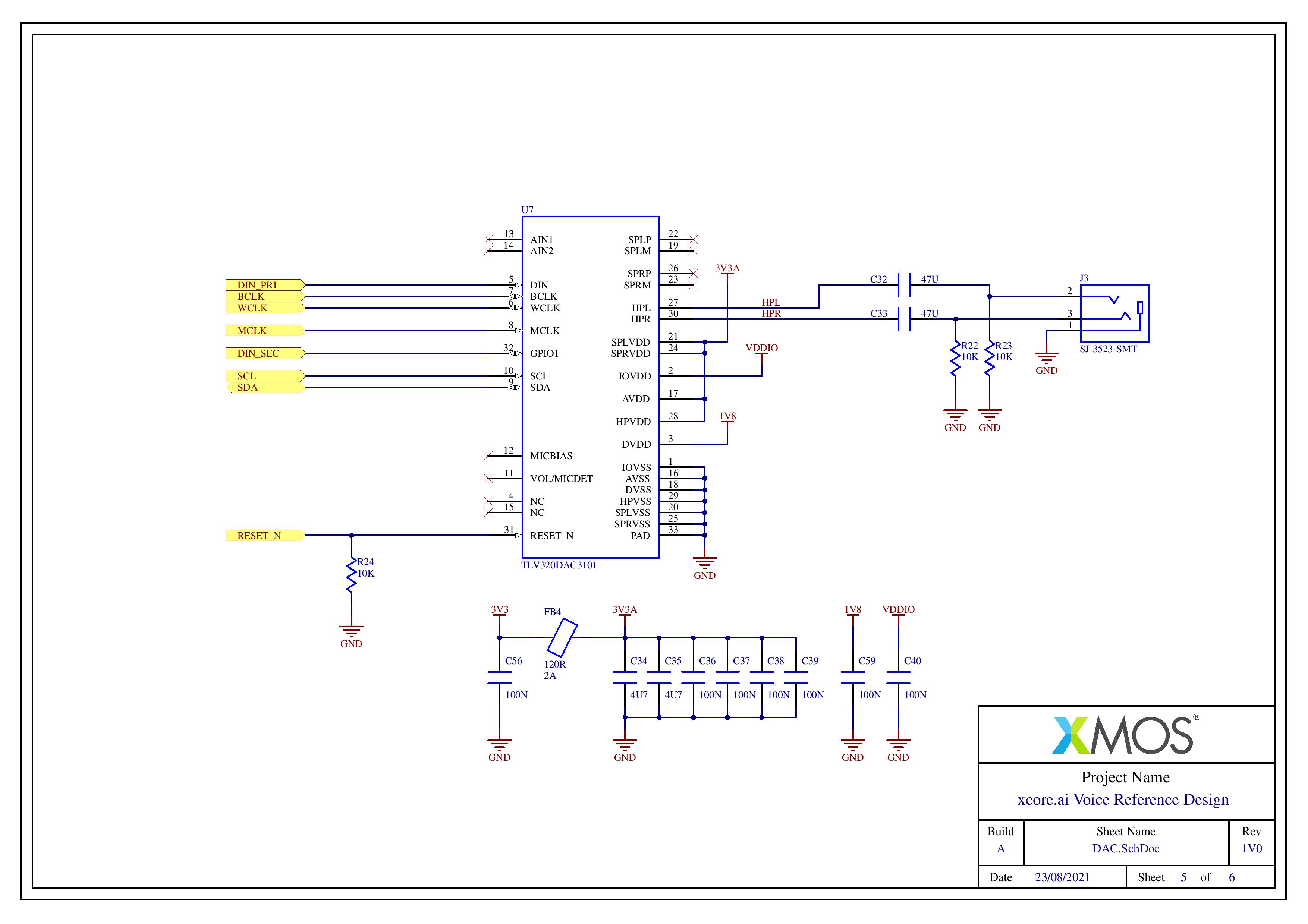
Fig. 11 XK-VOICE-L71 Schematic, page 5#
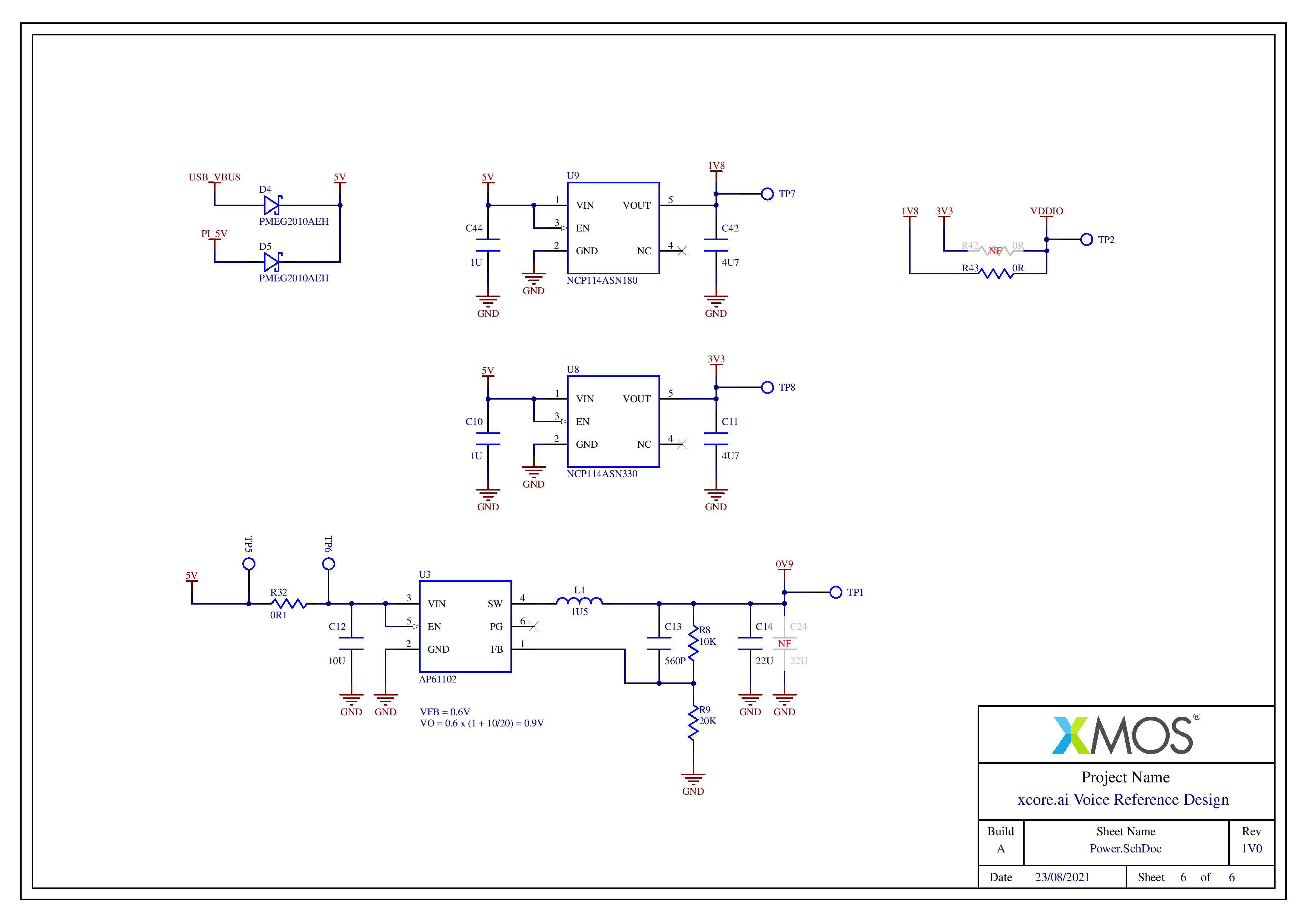
Fig. 12 XK-VOICE-L71 Schematic, page 6#
Bill of Materials#
This BOM is available as an Excel spreadsheet in the CAD data, available to Download
DESIGN |
XMS0001 |
||||
REVISION |
1V0 |
||||
VARIANT |
A |
||||
DATE |
23/08/2021 12:15:45 |
ITEM |
DESCRIPTION |
MANUFACTURER |
PART NUMBER |
QUANTITY |
DESIGNATOR |
|---|---|---|---|---|---|
1 |
Pin Header, Male, Vertical, Through Hole, 2 Way, 1x2, 0.1 Inch Pitch |
FCI |
68001-202HLF |
1 |
J2 |
2 |
USB Micro B Receptacle, Right Angle, SMD w/2 DIP Legs |
FCI |
10118193-0001LF |
1 |
J5 |
3 |
TRS jack, 3.5mm, SMD |
CUI |
SJ-3523-SMT |
1 |
J3 |
4 |
FFC/FPC Connector, 8 Way, 0.5mm Pitch, Slide Lock, Vertical, SMD |
Molex |
525590853 |
1 |
J9 |
5 |
Header, Female, Vertical, 40 Way, 2x20, 0.1 Inch Pitch, Locating Pegs, Bottom Entry, SMD |
Samtec |
REF-182665-01 |
1 |
J4 |
6 |
Box Header, Male, Vertical, Polarised, 20 Way, 2x10, 0.05 Inch Pitch, SMD |
Amphenol FCI |
20021521-00020T4LF |
1 |
J1 |
7 |
CHIP RESISTOR, 0.1 OHM, 100mW, 1%, 0603 |
Yageo |
RL0603FR-070R1L |
1 |
R32 |
8 |
CHIP CAPACITOR, CERAMIC, 47UF, 6.3V, 20%, X5R, 1206 |
Samsung |
CL31A476MQHNNNE |
2 |
C32, C33 |
9 |
CHIP CAPACITOR, CERAMIC, 10UF, 10V, 20%, X5R, 0603 |
Murata |
GRM188R61A106ME69 |
1 |
C12 |
10 |
CHIP CAPACITOR, CERAMIC, 22UF, 6.3V, 20%, X5R, 0603 |
Murata |
GRM188R60J226MEA0 |
1 |
C14 |
11 |
Ferrite Bead, 120R AT 100MHz, For Power Lines, 0603, 2A |
Murata |
BLM18PG121SN1 |
2 |
FB3, FB4 |
12 |
Ferrite Bead, 600R AT 100MHz, For GHz Noise, 0402, 0.3A |
Taiyo Yuden |
BKH1005LM601-T |
2 |
FB1, FB2 |
13 |
Power Inductor, 1.5uH, 2.6A, 65mR DCR, 2.5x2.0x1.2mm, SMD |
Taiyo Yuden |
MAMK2520H1R5M |
1 |
L1 |
14 |
Stereo Audio DAC, Low-Power, Headphone Amplifier, Stereo Class-D Speaker Amplifier, PLL, QFN32 |
Texas Instruments |
TLV320DAC3101IRHB |
1 |
U7 |
15 |
Processor, xcore.ai, 7x7mm 60QFN, 1200MIPS, 1.8V VDDIO |
XMOS |
XU316-1024-QF60A-C24 |
1 |
U2 |
16 |
8-bit I2C I/O Port, Agile IO, with interrupt and reset, TSSOP16 |
NXP |
PCAL6408APW |
1 |
U12 |
17 |
Bidirectional Voltage-Level Translator, Auto-Direction Sensing, 4 bit, UQFN-12 |
Texas Instruments |
TXB0104RUTR |
3 |
U10, U11, U13 |
18 |
Quad Logic Buffer, 3-state, LVC Series, VQFN14 |
NXP |
74LVC125ABQ |
1 |
U6 |
19 |
Memory, Flash, SPI, Multi-IO, 64Mb (32Kx256), 1.7 to 1.95V, QE = 1, SOIC-8-W |
Winbond |
W25Q64JWSSIQ |
1 |
U1 |
20 |
MEMS Microphone, Digital, PDM, Bottom Port, 69dB SNR, 4x3mm, LGA-5 |
Infineon |
IM69D130V01XTSA1 |
2 |
U100, U101 |
21 |
Voltage Regulator, Linear, Fixed, 3V3, 300mA, Output Active Discharge, TSOT23-5 |
ON Semiconductor |
NCP114ASN330T1G |
1 |
U8 |
22 |
Voltage Regulator, Linear, Fixed, 1V8, 300mA, Output Active Discharge, TSOT23-5 |
ON Semiconductor |
NCP114ASN180T1G |
1 |
U9 |
23 |
DC-DC Synchronous Buck Converter, Adjustable, PFM/PWM, Power Good, 2.2MHz, 1A, SOT563 |
Diodes Incorporated |
AP61102Z6-7 |
1 |
U3 |
24 |
Crystal, 24MHz, Freq Tol. ±10ppm, Freq Stab. ±10ppm, CL 10pF, Max ESR 80 Ohm, 2.0x1.6mm SMD |
Murata |
XRCGB24M000F1H02R0 |
1 |
X1 |
25 |
MOSFET, P-Channel, Logic Level, 20V, 2.4A, SOT23 |
ON Semiconductor |
NTR4101PT1G |
1 |
Q1 |
26 |
MOSFET, N-Channel, Logic Level, Gate-Source Protection, 25V, 220mA, SOT23 |
ON Semiconductor |
FDV301N |
1 |
Q2 |
27 |
ESD Protection Diode Array, 0.6pF, SC-70-6 (SC-88) |
ON Semiconductor |
NUP4114UCLW1T2G |
1 |
D6 |
28 |
Schottky Diode, 20V, 1.0A, SOD123F |
Nexperia |
PMEG2010AEH |
2 |
D4, D5 |
29 |
Dual MOSFET, N-Channel, Logic Level, Gate-Source Protection, 20V, 0.35A, SOT-563 |
Vishay Siliconix |
SI1024X-T1-GE3 |
1 |
Q3 |
30 |
LED, Top View, RED/GREEN, SMD, 0606 |
Lite-On |
LTST-C195KGJRKT |
1 |
D2 |
31 |
LED, Hyper Red, 0603 |
Kingbright |
APT1608SURCK |
1 |
D1 |
32 |
Tactile Switch, Momentary, 160gf, 2.5mm High, 4.2x3.2mm, J Bend SMD |
C&K |
PTS810SJM250SMTRLFS |
1 |
SW2 |
33 |
Sub Miniature Slide Switch, DPDT, 3.5mm High, 9.0x3.5mm, Right Angle, SMD |
C&K |
JS202011JAQN |
1 |
SW1 |
34 |
CHIP RESISTOR, ZERO OHM JUMPER, 1A, 0402 |
Yageo |
RC0402JR-070RL |
1 |
R43 |
35 |
CHIP RESISTOR, 33 OHM, 63mW, 1%, 0402 |
Yageo |
RC0402FR-0733RL |
2 |
R39, R40 |
36 |
CHIP RESISTOR, 100 OHM, 63mW, 1%, 0402 |
Yageo |
RC0402FR-07100RL |
4 |
R10, R13, R17, R44 |
37 |
CHIP RESISTOR, 330 OHM, 63mW, 1%, 0402 |
Yageo |
RC0402FR-07330RL |
1 |
R2 |
38 |
CHIP RESISTOR, 470 OHM, 63mW, 1%, 0402 |
Yageo |
RC0402FR-07470RL |
2 |
R16, R21 |
39 |
CHIP RESISTOR, 680 OHM, 63mW, 1%, 0402 |
Yageo |
RC0402FR-07680RL |
1 |
R7 |
40 |
CHIP RESISTOR, 1.0K OHM, 63mW, 1%, 0402 |
Yageo |
RC0402FR-071KL |
1 |
R20 |
41 |
CHIP RESISTOR, 4.7K OHM, 63mW, 1%, 0402 |
Yageo |
RC0402FR-074K7L |
4 |
R1, R3, R27, R28 |
42 |
CHIP RESISTOR, 6.8K OHM, 63mW, 1%, 0402 |
Yageo |
RC0402FR-076K8L |
2 |
R25, R26 |
43 |
CHIP RESISTOR, 10K OHM, 63mW, 1%, 0402 |
Yageo |
RC0402FR-0710KL |
15 |
R5, R8, R12, R19, R22, R23, R24, R29, R30, R31, R33, R34, R35, R36, R41 |
44 |
CHIP RESISTOR, 20K OHM, 63mW, 1%, 0402 |
Yageo |
RC0402FR-0720KL |
1 |
R9 |
45 |
CHIP RESISTOR, 47K OHM, 63mW, 1%, 0402 |
Yageo |
RC0402FR-0747KL |
3 |
R11, R15, R18 |
46 |
CHIP RESISTOR, 1.0M OHM, 63mW, 5%, 0402 |
Yageo |
RC0402JR-071ML |
1 |
R6 |
47 |
CHIP CAPACITOR, CERAMIC, 18PF, 50V, 5%, NP0, 0402 |
Yageo |
CC0402JRNPO9BN180 |
2 |
C3, C4 |
48 |
CHIP CAPACITOR, CERAMIC, 100NF, 16V, 10%, X7R, 0402 |
Yageo |
CC0402KRX7R7BB104 |
41 |
C1, C5, C6, C7, C8, C9, C16, C17, C18, C19, C20, C21, C22, C23, C25, C27, C28, C29, C30, C31, C36, C37, C38, C39, C40, C41, C43, C45, C46, C47, C48, C49, C50, C51, C52, C53, C54, C55, C56, C58, C59 |
49 |
CHIP CAPACITOR, CERAMIC, 1.0UF, 16V, 10%, X5R, 0402 |
Murata |
GRM155R61C105MA12D |
6 |
C2, C10, C15, C26, C44, C57 |
50 |
CHIP CAPACITOR, CERAMIC, 560PF, 50V, 5%, NP0, 0402 |
Yageo |
CC0402JRNPO9BN561 |
1 |
C13 |
51 |
CHIP CAPACITOR, CERAMIC, 4.7UF, 16V, 10%, X5R, 0603 |
Murata |
GRM188R61C475KE11D |
4 |
C11, C34, C35, C42 |
NA |
NO FIT COMPONENTS |
NA |
NA |
0 |
J8, J7, J6, C24, R14, R37, R38, R42, R45, R4 |